关于LatticeMico8
The LatticeMico8 is an 8-bit microcontroller optimized and fully tested for the MachXO2™ family of Programmable Logic Devices (PLDs). It can also be used as a reference design for the other families of Field Programmable Gate Arrays (FPGAs). Combining a full 18-bit wide instruction set with 32 general purpose registers, the LatticeMico8 is suitable for a wide variety of markets, including communications, consumer, computer, medical, industrial, and automotive. The core consumes minimal device resources, less than 200 Look Up Tables (LUTs) in the smallest configuration, while maintaining a broad feature set.
The LatticeMico8 is licensed under a new open intellectual property (IP) core license, the first such license offered by any FPGA supplier. The main benefits of using open source IP are greater flexibility, improved portability, and no cost. This new agreement provides all the benefits of standard open source and allows users to mix proprietary designs with the open source core. Additionally, it allows for the distribution of designs in bitstream or FPGA format without accompanying it with a copy of the license.
开发工具
LatticeMico System is to be used to implement a LatticeMico8 micro-controller system with attached peripheral components. It is based on the Eclipse C/C++ Development Tools environment, which is an industry open-source development and application framework for building software.
特色
- Innovative Open IP Core License
- Efficient Architecture and Broad Feature Set
- 18-bit Wide Instructions
- Configurable 16 or 32 General Purpose Registers
- Configurable Instruction Memory (PROM)
- Internal or external through Wishbone Interface
- Configurable to accomodate 256, 512, 1K, 2K or 4K instructions
- Scratchpad Memory
- Internal or external through Wishbone Interface
- Configurable up to 4 Gigabytes using paging (256 bytes per page)
- Mimimum two cycles per instruction
- Configurable 8, 16, or 32-deep call stack
- Support for up to 8 external interrupts
- Integrated hardware loader to optionally initialize PROM and Scratch pd for an external non-volatile mem
- Wishbone Peripheral Components:
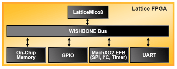
- GPIO, UART, DMA Controller, SPI Flash Controller, MachXO2 EFB (I2C, SPI, Timer)
框图
性能和所占资源
Config. Number Description Device LUTs Registers f MAX (MHz) 1 16 - Regs, data & I/O addressable range 256, 8-Call Stack depth, 512 PROM, 32 byte Int SP LCMXO2-1200HC-5T G100C 194 83 46.2 2 32 - Regs, data & I/O addressable range 256, 8-Call Stack depth, 512 PROM, 32 byte Int SP LCMXO2-1200HC-5T G100C 206 83 49 3 16 - Regs, data & I/O addressable range 256, 8-Call Stack depth, 512 PROM, 16 byte Int SP LCMXO2-1200HC-5T G100C 193 83 48 4 32 - Regs, data & I/O addressable range 256, 8-Call Stack depth, 512 PROM, 16 byte Int SP LCMXO2-1200HC-5T G100C 205 83 52.2 SP = Scratch Pad
1These numbers may vary as you change the operating conditions.
相关文档
- 快速参考技术资源
- 应用指南
- 用户手册
- 参考设计
- 产品手册
- 教程


