低压差或LDO稳压器是一种能够在输入电压很接近输出要求电压的情况下也能够保持稳压的直流线性稳压器。相较于其他的直流-直流稳压器其优点是没有开关噪声(没有开关过程)、器件体积较小(不需要大电感或变压器),设计极其简单;最大的缺点是线性直流稳压器必须在器件上以发热的方式消耗能量以保证输出电压的稳定。
来历
可调节输出的低压差线性稳压器最早于1977年4月12日发布,标题为“Break Loose from Fixed IC Regulators“文章,作者是大名鼎鼎的Robert Dobkin,当时他在美国国家半导体公司(National Semiconductor)做IC设计师,由此美国国家半导体公司宣称自己是“LDO的发明者”。 Dobkin于1981年离开美国国家半导体公司创办了Linear Technology公司,目前他还任Linear Technology的CTO。
器件
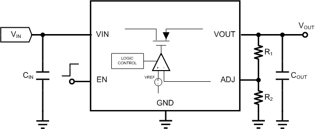
LDO的原理示意图
主要的器件是一个功率FET和一个差分放大器(误差放大)。差分放大器的一个输入端监测由输出电压经取样电阻R1/R2的比率决定的输出,另一个输入端连接一个稳定的电压基准源。如果输出电压相对于参考电压升的太高,则驱动功率FET以保持一个稳定的输出电压。
稳压
LDO和其它的线性稳压器工作模式是一样的,LDO和非LDO的稳压器的主要区别在于它们的原理拓扑结构,LDO采用了集电极开路或漏极开路的方式,而不是一个发射极跟随的方式。采用这种结构稳压器上的电压很容易驱动晶体管进入饱和状态,这就使得从待稳定的电压到稳定的输出电压之间的压差可以低到晶体管上的饱和电压。
如上图,输出电压为:
V{OUT}= \left( 1 + \frac{R1}{R2} \right) V{REF}
如果采用的是三极管,而不是场效应管或JFET,为控制它需要比较大的附加能量,非LDO会自身消耗掉压降导致的能量,For high voltages under very low In-Out difference there will be significant power loss in the control circuit.
因为功率控制的部分起到逆变器的作用,需要另外一个逆变的放大器来控制它,这样相对于普通的线性稳压器就增加了电路的复杂度。
一般选用功率FET来降低功耗,但这在输入电压比较低的时候也会带来问题,因为FET一般需要5-10V才能彻底关断,功率FET也会导致成本增加。
效率和散热
The power dissipated in the pass element and internal circuitry (P_{LOSS}) of a typical LDO is calculated as follows:
P\text{LOSS} = ( V\text{IN} - V\text{OUT} ) \times I\text{OUT} + ( V\text{IN} \times I{Q} )
where I_{Q} is the quiescent current required by the LDO for its internal circuitry.
Therefore, one can calculate the efficiency as follows:
\eta = \frac{P\text{IN} - P\text{LOSS}}{P\text{IN}} where P\text{IN} = V\text{IN} \times I\text{OUT}
However, when the LDO is in full operation (i.e., supplying current to the load) generally: I\text{OUT} » I\text{Q}. This allows us to reduce P_\text{LOSS} to the following:
P\text{LOSS} = ( V\text{IN} - V\text{OUT} ) \times I\text{OUT}
which further reduces the efficiency equation to:
\eta = \frac{V\text{OUT}}{V\text{IN}}
It is important to keep thermal considerations in mind when using a low drop-out linear regulator. Having high current and/or a wide differential between input and output voltage could lead to large power dissipation. Additionally, efficiency will suffer as the differential widens. Depending on the package, excessive power dissipation could damage the LDO or cause it to go into thermal shutdown.
静态电流
Among other important characteristics of a linear regulator is the quiescent current, also known as ground current or supply current, which accounts for the difference, although small, between the input and output currents of the LDO, that is:
I{Q} = I{IN} - I_{OUT}
Quiescent current is current drawn by the LDO in order to control its internal circuitry for proper operation. The series pass element, topologies, and ambient temperature are the primary contributors to quiescent current.[6]
Many applications don't require an LDO to be in full operation all of the time (i.e. supplying current to the load). In this idle state the LDO still draws a small amount of quiescent current in order to keep the internal circuitry ready in case a load presented. When no current is being supplied to the load, P_{LOSS} can be found as follows:
P{LOSS} = V{IN} \times I_{Q}
滤波
Torex XC6206 3.3V LDO voltage regulator in SOT23-3 package In addition to regulating voltage, LDOs can also be used as filters. This is especially useful when a system is using switchers, which introduce a ripple in the output voltage occurring at the switching frequency. Left alone, this ripple has the potential to adversely affect the performance of oscillators,[7] data converters,[8] and RF systems[9] being powered by the switcher. However, any power source, not just switchers, can contain AC elements that may be undesirable for design.
Two specifications that should be considered when using an LDO as a filter are power supply rejection ratio (PSRR) and output noise.
指标
评价一个LDO主要的指标有:
- 电压差
- 静态电流
- 负载调整率
- 线调整率
- 最大电流(取决于导通晶体管的大小)
- 对负载变化的响应速度
- 由于负载电流的突变、输出电容以及等效的串行阻抗对输出电压的影响
电源抑制比
PSRR refers to the LDO's ability to reject ripple it sees at its input.[11] As part of its regulation, the error amplifier and bandgap attenuate any spikes in the input voltage that deviate from the internal reference to which it is compared.[12] In an ideal LDO, the output voltage would be solely composed of the DC frequency. However, the error amplifier is limited in its ability to gain small spikes at high frequencies. PSRR is expressed as follows:[11]
PSRR = 20 \times log \frac{Ripple{IN}}{Ripple{OUT}}
As an example, an LDO that has a PSRR of 55 dB at 1 MHz attenuates a 1 mV input ripple at this frequency to just 1.78 µV at the output. A 6 dB increase in PSRR roughly equates to an increase in attenuation by a factor of 2.
Most LDOs have relatively high PSRR at lower frequencies (10 Hz - 1 kHz). However, a Performance LDO is distinguished in having high PSRR over a broad frequency spectrum (10 Hz - 5 MHz). Having high PSRR over a wide band allows the LDO to reject high-frequency noise like that arising from a switcher. Similar to other specifications, PSRR fluctuates over frequency, temperature, current, output voltage, and the voltage differential.
输出噪声
LDO自身产生的噪声也应该被考虑在滤波器的设计中,与其它电子器件一样,LDO也受到热噪声、双极散射噪声、以及闪变噪声的影响。所有这些噪声叠加在一起影响了输出的电压,这些噪声主要分布在低频段。为了滤除交流频率,在输入端和输出断都要进行纹波抑制。
负载稳压
Load regulation is a measure of the circuit’s ability to maintain the specified output voltage under varying load conditions. Load regulation is defined as:
Load Regulation = {\Delta V{OUT} \over \Delta I{OUT}}
The worst case of the output voltage variations occurs as the load current transitions from zero to its maximum rated value or vice versa.[6]
Line regulation
Line regulation is a measure of the circuit’s ability to maintain the specified output voltage with varying input voltage. Line regulation is defined as:
Line Regulation = {\Delta V{OUT} \over \Delta V{IN}}
Like load regulation, line regulation is a steady state parameter—all frequency components are neglected. Increasing DC open-loop current gain improves the line regulation.[6]
Transient response
The transient response is the maximum allowable output voltage variation for a load current step change. The transient response is a function of the output capacitor value ({\textstyle C{OUT} }), the equivalent series resistance (ESR) of the output capacitor, the bypass capacitor ({\textstyle C{BYP} }) that is usually added to the output capacitor to improve the load transient response, and the maximum load-current ({\textstyle I_{OUT,MAX} }). The maximum transient voltage variation is defined as follows:
\Delta V{TR,MAX} = {I{OUT,MAX} \over {C{OUT}+C{BYP}} } \Delta t{1} + \Delta V{ESR} [6]
Where {\textstyle \Delta t{1} } corresponds to the closed-loop bandwidth of an LDO regulator. {\textstyle \Delta V{ESR} } is the voltage variation resulting from the presence of the ESR ({\textstyle R_{ESR} }) of the output capacitor. The application determines how low this value should be.
