关于LatticeMico32
The LatticeMico32™ is a 32-bit Harvard, RISC architecture “soft” microprocessor, available for free with an open IP core licensing agreement. The LatticeMico32 provides the visibility, flexibility and portability that you expect in an open source hardware design. Everything you need is provided, including software development tools (via LatticeMico™ System) and evaluation boards to try out your designs in hardware.
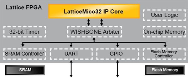
By combining a 32-bit wide instruction set with 32 general purpose registers, the LatticeMico32 provides the performance and flexibility suitable for a wide variety of markets. Using a RISC architecture, the core consumes minimal device resources, while maintaining the performance required for a broad application set. To accelerate the development of microprocessor systems, several optional WISHBONE compatible peripheral components may be integrated with the LatticeMico32.
兼容WISHBONE的外设部件
To accelerate the development of microprocessor systems, several optional WISHBONE compatible peripheral components may be integrated with the LatticeMico32.
- Memory controllers
- DDR, DDR2 & DDR3 SDRAM
- Asynchronous SRAM
- On-chip Block Memory
- SDRAM controller
- On-chip dual port memory
- SPI Flash
- Parallel Flash
- I/O
- 32-bit Timer
- DMA Controller
- GPIO
- I2C Master Controller
- SPI
- Tri-Speed Ethernet MAC
- UART
- PCI Target
Three Configurations to Optimize Area and Performance
- Basic
- No Multiplier
- Multicycle Shifter
- No Cache
- Standard
- Multiplier
- Pipelined Shifter
- 8K I-Cache, No D-Cache
- Full
- Multiplier
- Pipelined Shifter
- 8K I-Cache, 8K D-Cache
开发工具
LatticeMico System is to be used to implement a LatticeMico32 system with attached peripheral components. It is based on the Eclipse C/C++ Development Tools Environment, which is an industry open-source development and application framework for building software.
特性
- Optimized for Lattice FPGA Devices
- Performance Enhanced Feature Set
- RISC architecture
- 32-bit data path and 32-bit instructions
- 32 general purpose registers
- Handles up to 32 external interrupts
- Optional instruction and data caches
- Dual WISHBONE memory interfaces (Instruction and Data)
框图
性能和所用资源
Performance and Resource Utilization1 Lattice FPGA Family Configuration LUTs fMAX (MHz) LatticeECP3 Standard 2,370 115 LatticeXP2TM Standard 2,406 85 LatticeECP2/M Standard 2,497 110 1Performance and utilization characteristics are generated using Lattice Diamond software. When using the LatticeMico32 in a different density, speed, or grade within the Lattice FPGA family, performance may vary.


